
The development of compact embedded systems is essential to make the excellent SPAD features truly within the reach of end users. It is worth saying that experts of the various applications that benefit from SPAD exploitation need powerful yet easy-to-use systems, thus often requiring a tailored design. Above all, to fully support the extraordinary performance that can be extracted from custom SPADs and dedicated integrated electronics, it is necessary to have a solid and reliable on-board system.
Indeed, the integrated circuits can easily produce fast pulses and data rates in the order of hundreds of MHz, or even higher, which could impair the overall performance of the system because of crosstalk, induced disturbances, ground bounces, fluctuations of voltage power supply and so on. Moreover, custom SPADs often have requirements which are challenging to combine. For example, high bias voltages are necessary to bias the SPAD above its breakdown, but high stability of the power supply is also necessary to preserve the precious timing information produced by the front end and the TAC (see Integrated electronics section). Furthermore, custom SPADs feature a significant dependence of their performance from the operating temperature, a characteristic that can be exploited to reduce the noise by cooling down the device below 0°C.
While relatively simple solutions can be used with single channel systems, the recent availability of dense SPAD arrays poses new challenges in the design of systems able to extract high performance.
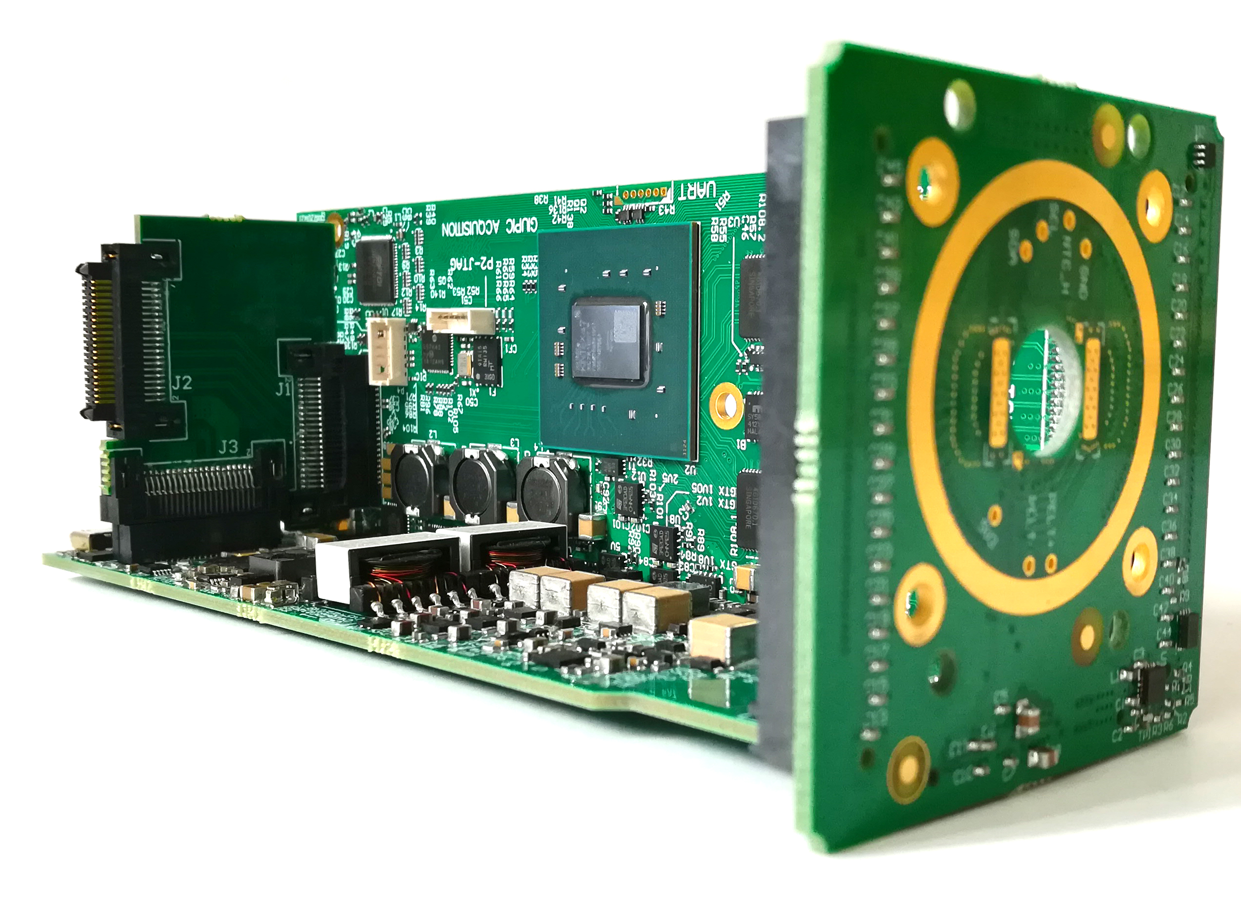
To have an idea, SPAD arrays and integrated electronics can dissipate up to few Watts of power in few cm2 of area, making the power dissipation density a critical aspect in the embedded system design that need to be addressed with complex solutions as multi-stage thermoelectric coolers (like Peltier cells) and temperature control feedback to constantly monitor and adjust the temperature gradient of the chip. When it comes to large SPAD arrays, both for counting and timing applications, on-board signal routing, processing and data transmission toward an elaboration unit require system architectures developed on purpose and an efficient exploitation of resources by means of dedicated firmware. In our lab, we address these challenges by designing high-performance PCBs (Printed Circuit Boards) including power supply generation and distribution, temperature control, data extraction and conversion using different logic families, both single ended (NIM, TTL, etc..) and differential (PECL, LVDS, ecc..). Moreover, we select the most appropriate components to enhance the capabilities of the system for each application, including Field Programmable Gate Arrays (FPGAs), such as Kintex-7 family, Sistem-On-Chip (SoC), like Zynq-7000, and microcontrollers (μC).
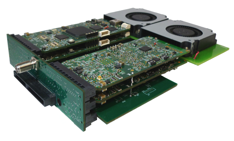
Coding provides us the degrees of freedom necessary to customize the system for each application. Furthermore, we address data processing and communication with external storage and elaboration units. In particular, the need to export huge quantities of data requires the implementation, both on hardware and on software, of fast transmission protocols, such as USB 3.0, camera link, optical link (10 Gbps) and ethernet (1 Gbps). To this aim, we make an extensive use of CAD software (Altium), programming software (Vivado with VHDL code, visual studio with C#, MPlab with C, Labview …) and laboratory instrumentations (oscilloscope, voltmeter, bench power supply, etc…). Last but not least, mechanical aspects are carefully addressed to design fully reliable modules.
Applications
In our lab we design embedded system for various applications and scopes, including but not limited to:
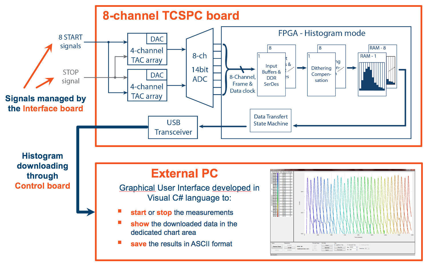
Fluorescence Lifetime Imaging (FLIM): TCSPC (Time Correlated Single Photon Counting) is a powerful yet somehow slow tool for FLIM experiments. A reduction by one or even two orders of magnitude of the time needed to perform a FLIM measurement would be a real breakthrough in many fields, especially in medicine and biology. For this reason, in recent years we investigated new solutions to design faster FLIM acquisition systems. On one hand, we demonstrated that increasing by one order of magnitude the speed of a single TCSPC channel, without distortion, is possible with a fine tuning of the SPAD dead time. Following the theoretical demonstration, we recently developed the first prototype that implements the new proposed technique. At the same time, we investigated the best way to use SPAD arrays, in order to combine high performance and high speed. To this aim, we developed a routing architecture that allows us to exploit the data transfer bandwidth at its best potential. Our current research is focused on the study and design of new electronics to combine these two aspects (single fast channel and arrays) into a system able to change the paradigm of TCSPC measurements.
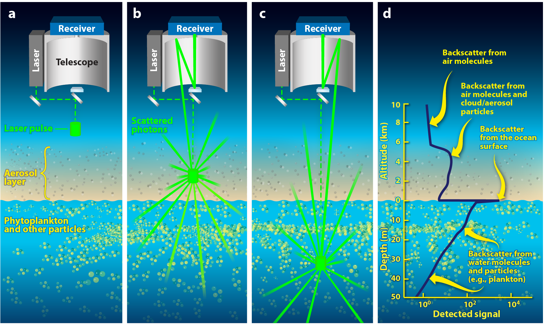
Spaceborne Lidar: light detection and ranging (lidar) sensors hosted on satellites have provided a valuable insight into the Earth’s surface and atmosphere. Nevertheless, currently-available acquisition systems lack the performance necessary to capture the details of cloud tops and ocean phytoplankton to a fidelity sufficient for advancing our understanding of mechanisms involved in climate changing. Custom, densely integrated SPAD arrays, combined with fast integrated electronics able to provide quenching and reset times within 10ns, promise to enable new measurements, while also offering a sensitivity that will allow significant reductions in laser power and telescope size, with associated savings in weight and power that are crucial for spaceborne-suitable design. In our lab, we recently developed a prototype in collaboration with NASA Research Center to prove the validity of a new acquisition scheme based on our SPAD arrays for this application. Next steps include the design of both new integrated electronics and embedded systems to scale up our solution to hundreds of SPADs and to make the system compliant with space requirements, including radiation hardness.
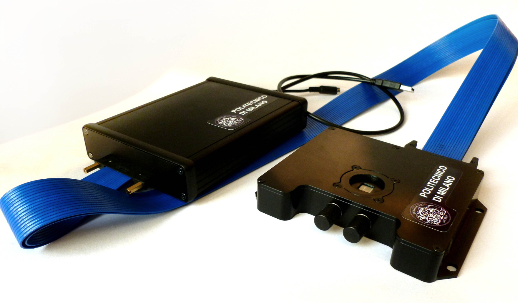
Systems to test integrated electronics: when a foundry delivers the chip, we need to carry out extensive tests and verify its behaviour and performance before it can be exploited in the final system. To this aim, we make us of both commercial evaluation boards and custom test boards developed on purpose. In this way, we have the degrees of freedom necessary to deeply test the chip, also in extreme situations, by controlling each input and output individually. With respect to application PCBs, test boards can be easier to design and faster to implement, mainly because of limited number of components and less stringent area constraints, but they can still represent a challenge for the designer that needs to conceive the proper validation tests for each chip.
Verification and validation of algorithms later implemented in integrated circuits: implementing new logic functions and algorithms directly into integrated chips can be very time-consuming and economically expensive. For these reasons, we exploit FPGAs and μCs as prototyping platforms to implement new algorithms. This approach gives us the degrees of freedom to verify the algorithm’s validity and functionality before we consider its fully-integrated implementation.