
Avalanche simulation
One of the best features of SPADs is their ability to not only detect single photons, but to also provide the information about the time of arrival of each photon with picosecond precision. To predict the timing performance of designed SPADs, both single pixels and arrays, and to understand how to push this performance beyond the current state of the art, a deep understanding of the physical mechanisms that regulate the charge transport in the device, with particular focus on the impact ionization, is crucial. For this reason, our lab is involved in broad-spectrum physical modeling.
Our study starts from the analysis of transport mechanisms, considering the complete band structure of the silicon and the real quantum scattering coefficients. The problem relates to the solution of the Boltzmann transport equation (BTE) both by means of analytical techniques (such as SHE or HARM) and statistical techniques such as the Full-Band Monte Carlo (FBMC). From this type of analysis, the main physical parameters necessary to the construction of some simplified models of the Kinetic Monte-Carlo (KMC) type are extracted, which allow us to carry out the simulation of the entire device in different operating conditions (bias, front-end electronics load, etc…) and, above all, with different manufacturing parameters (type and doping profile, epitaxial layers, etc …).
In recents years, we developed models which allowed us to study the triggering of the avalanche from the early stages with time scales that can reach the femtosecond. The numerical results are always compared with data extracted from the experimental characterization, potentially involving some ad-hoc measurement techniques, in order to validate and refine our models. The deep awareness of the physical phenomena involved with SPAD behavior that we gained through the development, simulation and validation of physical models has allowed us to develop and implement new, cutting-edge devices capable of pushing SPAD performance beyond the current state of the art.
Optical crosstalk
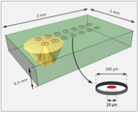
Moreover, in recent years there has been a growing interest in monolithic SPAD arrays, as they open the way to advanced and multi-parameter analysis (wavelength, spatial distribution, temporal distribution, etc..) of weak and/or ultra-fast light signals (see System section). To meet the high-demanding requirements of various applications, it is decisive to understand the physical limits imposed by the coexistence of multiple SPADs on the same silicon die as long as the ultimate limit of the miniaturization process.
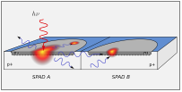
For example, a potential limitation to the integration of multiple SPADs in a monolithic array is due to the photon emission occurring during the avalanche process. Indeed, when an avalanche is triggered in a pixel due to the absorption of a primary (signal) photon, some secondary photons are emitted by the pixel itself. These photons propagating inside the chip can cause the triggering of avalanches in other pixels of the array, thus causing crosstalk between the photodetectors. Such optical crosstalk can not only lead to an incorrect evaluation of the signal incident on each SPAD of the array, but it can also limit the dynamic range of the entire array. Since the intensity of the optical crosstalk increases by reducing the distance between the pixels, this phenomenon represents an important limit to the integration density of the array. Moreover, a deep investigation of crosstalk phenomena has been systematically addressed in our lab by both experimental characterization of different fabrication slots and test structures and by studying the physical mechanisms that can determine this effect. This combined approach has allowed us to realize that the observed dependence of crosstalk on SPAD distance could not be simply ascribed to a direct propagation of photons from one SPAD to another, thus suggesting that a significant role can be also played by indirect optical paths.
This theory, proposed for the first time by our research group, has been confirmed by a series of experimental tests which have therefore allowed us to validate its correctness. Showing that a considerable contribution to optical crosstalk in SPAD arrays can be given by optical paths that undergo one or more reflections off the bottom of the chip has allowed us not only to obtain an optical model in excellent agreement with experimental data, but it also gave us a powerful tool to design new generations of SPAD arrays in which optical crosstalk is to be minimized.