

The design of cutting-edge integrated front-end and processing electronics is paramount to fully unlock the potential of custom Single Photon Avalanche Diodes (SPADs).First and foremost, the front-end electronics is directly connected to the sensor: its rapidity to quench the avalanche current and reset the device plays a key role to asses the speed, the power dissipation and the correlated noise of the whole system. Moreover, SPADs can provide the information about the time of arrival of each photon with picosecond precision. To this aim, not only an avalanche current pick-up circuit is required, capable of combining a high bandwidth, a low sensing threshold and a low crosstalk when used in arrays, but also a picosecond-precision time-measurement circuit able to convert such information into digital data. Last but not least, on-chip data processing and routing is crucial to extract the information from densely integrated systems. For all these reasons, the research of our lab on integrated electronics sweeps from analog transistor-level design to fast and compact digital circuits and mixed-signal electronics. Our current focus is mainly on the following areas:
Quenching/reset and timing front-end
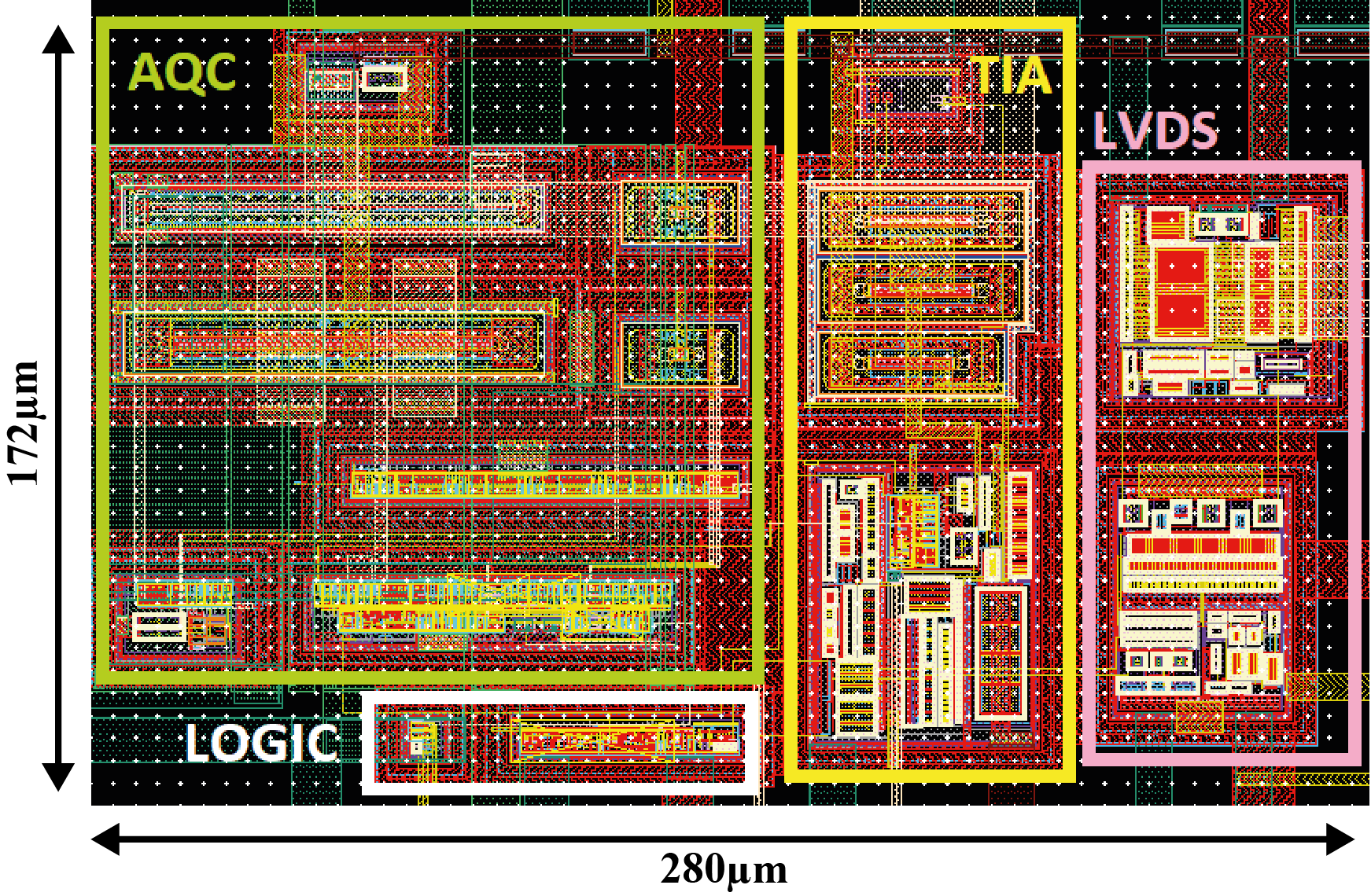
Since the beginning, the use of a SPAD has been possible thanks to the quenching/reset circuit,which is in charge of interrupting the avalanche current (quenching phase) and restoring the initial bias conditions (reset phase) to make the SPAD ready to detect another photon. Although the basic principle of operation is well known in the field, the design of a quenching/reset circuit to achieve high-performance is still a challenging topic, especially with SPAD arrays. In our lab, we resort to a high-voltage CMOS technology to design AQCs for different SPADs and various applications, ranging from single molecule spectroscopy to spaceborne lidar.Furthermore, SPADs can provide the information about the arrival time of the photon with picosecond precision. To achieve this result, a wide-bandwidth and low-threshold current-sensing circuit is necessary. While such circuit can be easily designed for a single channel system, the integration of multiple channels in an array poses several challenges in terms of area occupation, power dissipation and crosstalk. Our research is currently focused on the design of avalanche-current pick-up circuits featuring large bandwidth and high-precision, and the possibility to be joined with quenching/reset capabilities to enable the design of densely integrated systems based on high-performance SPAD arrays.
Time measurement circuit
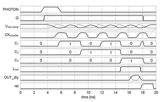
The analog information about the arrival time of a photon is contained in the onset of the SPAD avalanche current. To make available such information to any elaboration unit (FPGA, GPU, CPU, etc), a time to digital conversion is necessary.
In our lab, we follow an approach based on a fully-integrated time to amplitude converter (TAC) followed by an ADC. The TAC is the core of the time conversion process: its precision, linearity and speed set the performance of the overall system. Resorting to a BiCMOS technology, we are constantly working to push the precision beyond the state of the art in this field, while boosting the count rate to speed up the measurements, and keeping the non linearity to extremely low levels to fulfill the requirements of most demanding applications. To this aim, transistor-level low-noise design is combined with architectural design thinking.
Routing and data extraction electronics
The extraordinary progress in SPAD design and fabrication occurred in recent years has posed new challenges in the field. Above all, the possibility to integrate hundreds, or even thousands of sensors on the same silicon die can easily lead to the generation of a huge amount of data that need to be extracted, possibly stored and eventually processed. In our lab, we search for innovative and application-tailored solutions that allow us to design densely integrated systems featuring the highest performance that can be obtained with SPADs. To this aim, the integrated circuit designers work side-by-side with system engineers to embed the complexity wherever is more advisable to maximize the potential of the resulting instrumentation. For example, to advance the field of spaceborne lidar, we are working on the design of new systems able to count the number of photons impinging on large arrays of SPADs during time bins of few nanoseconds. To this aim, we need to be able to manage data rates that can easily reach the gigacount/s range. Such an ambitious goal requires integrated electronics to design very fast circuits able to collect data from dense SPAD arrays, overcoming interconnection, speed, and crosstalk issues. Moreover, several applications, especially in the biological field, need to mark the time of arrival of each photon with picosecond precision.Exploiting the peculiar features of each of those applications, we are working on new solutions that could allow us to boost the speed of each SPAD and/or share the resources among many detectors in order to optimize the overall performance of the system. In particular, we have been following an approach based on the extraction of the only data that can be effectively transferred to an external storage and/or elaboration unit, thus confining the most complexity at the earliest stage of the acquisition chain. To this aim, not only a dedicated, fast logic is necessary, but also a circuit able to preserve the precious timing information during the time needed make any decision required by the sharing mechanism.