
Introduction
The Single Photon Avalanche Diode (SPAD) is a photodetector capable of detecting a single photon by exploiting the avalanche phenomenon. Essentially, a SPAD is a pn junction reverse-biased above the breakdown voltage. However, unlike a common diode, in this condition the SPAD is not crossed by a strong current; on the contrary, it is in a metastable state characterized by a substantially zero current. When a photon is absorbed in the active area, an electron-hole pair is generated. The two photogenerated carriers are separated and accelerated by the electric field present in the space-charge region and they can free other carriers by impact ionization. The process is self-sustaining and it gives rise to a macroscopic current that can be easily detected by an external circuit. It is worth noting that once the avalanche has been triggered, the absorption of an additional photon does not cause any substantial change in the behavior of the device: the detector is therefore blind. For this reason, it is necessary to use suitable circuits to stop the avalanche and bring the device back to optimal working conditions (see “Integrated electronics” section). Unfortunately, the absorption of a photon is not the only phenomenon that can trigger an avalanche. Above all, thermal generation (Shockley Read and Hall theory – SRH) associated with the presence of trap states located within the gap can initiate the avalanche process. This and other phenomena determine “false clicks” of the detector that can occur even in absence of light, hence the name of dark counts. Their contribution represents the noise of a SPAD and must be therefore minimized.
Photon Counting and Photon Timing
The absorption of a photon by a SPAD is typically marked by a voltage or current signal produced by the quenching circuit. By counting the number of pulses generated in a given time interval, it is possible to trace the number of incident photons and therefore the optical power reaching the detector. This technique, called Photon Counting, is used more and more frequently to detect particularly weak optical signals in various applications. It is worth noting that the operating principle is quite different from the one of a classic photodetector: in the latter, an analog signal is generated, whose amplitude is proportional to the incident power. On the contrary, in Photon Counting the information does not lie in the amplitude of the signal, but in the number of pulses occurred in a fixed time window. This “digital” approach can easily make the noise introduced by the electronics irrelevant.
Moreover, SPADs can also provide the information about the arrival time of the photon. Such feature is exploited in Photon Timing. Exploiting the synchrony between the absorption of the photon and the subsequent emission of an electrical pulse, Photon Timing techniques have been conceived. In particular, Time Correlated Single Photon Counting (TCSPC) allows the reconstruction of the shape of ultra-fast optical signals, overcoming the bandwidth limitations of analog techniques. Indeed, the main advantage of TCSPC is that the temporal resolution is only limited by the jitter of the detector, or by the statistical fluctuation of the delay between the instant of absorption of the photon and the instant of generation of the pulse (see the Modeling section). Currently-available devices, combined with suitable electronics for reading the avalanche current, can provide a temporal resolution down to 20-30 ps.
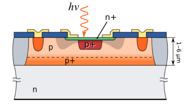
Design of SPAD detectors
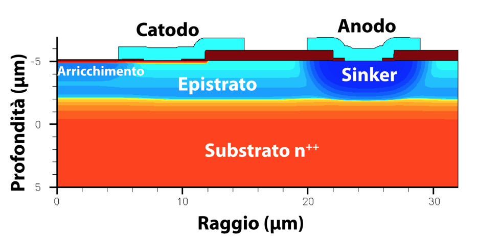
In recent years, the SPAD has been widely used in various application fields ranging from biology to chemistry, from genetics to astronomy, from non-invasive testing of integrated circuits to quantum cryptography. However, these applications require a continuous improvement of the detector’s performance which can only be obtained with a deep understanding and modeling of the physical phenomena that regulate its behavior. In our lab at Politecnico di Milano, we design custom SPADs using both commercial simulators and models developed on purpose. In particular, a process simulator allows us to predict the real structure of the device (geometry and doping profiles) starting from the detailed description of its fabrication steps (duration and temperature of the heat treatments, dopant implant doses, etc. …). The resulting structure can be used as input for another software, i.e the device simulator, which allows us to obtain various electrical parameters of the detector, such as the distribution of electrons and holes, the electric field profile, etc … Finally, specifically developed models allow us to infer the main performance of the detector (quantum efficiency, temporal resolution, etc …) that can be obtained with the designed structure. Overall, the combination of these tools allows the device designer to design and optimize new structures, evaluating their impact on the detector’s performance even before its physical fabrication.
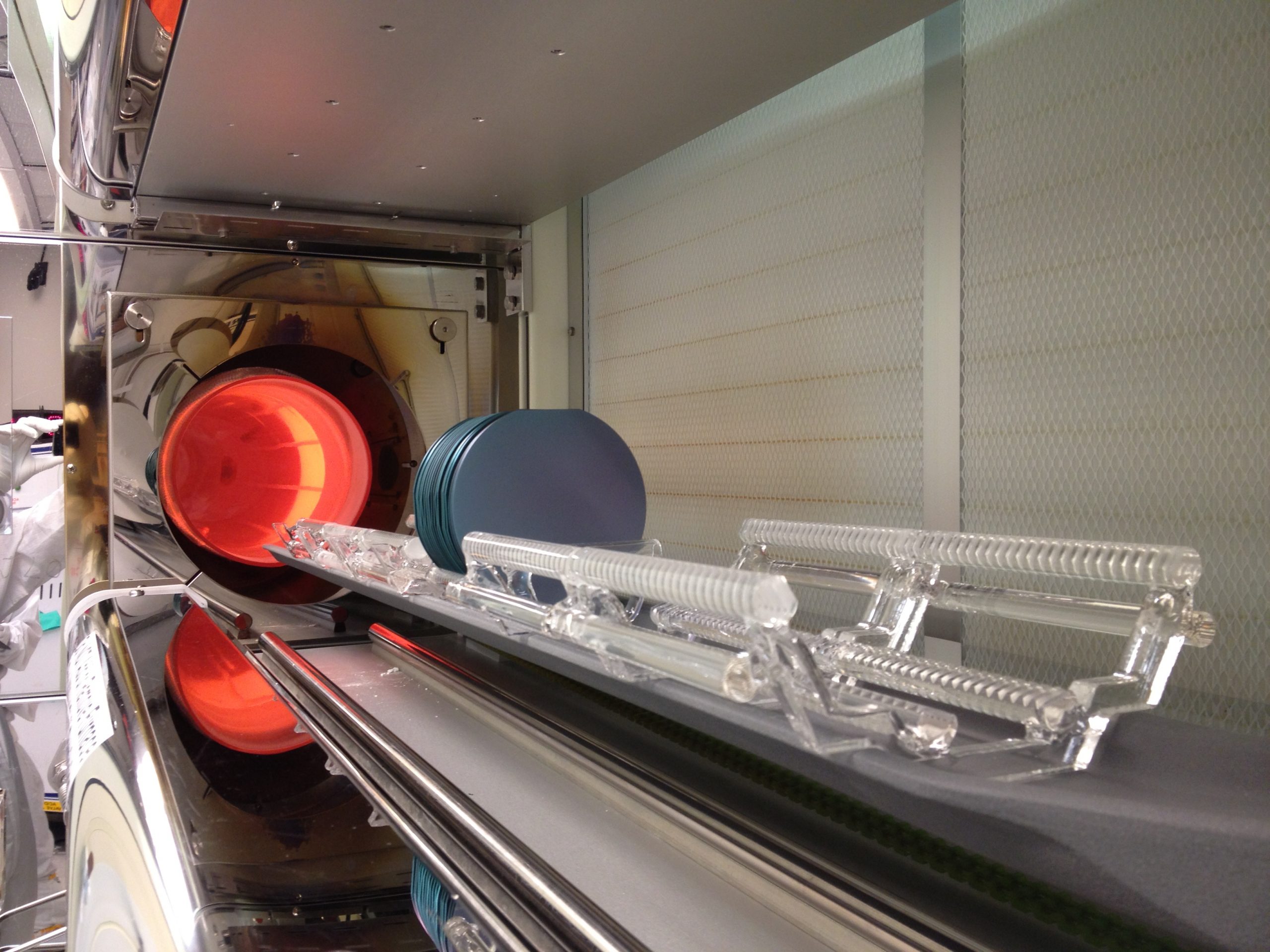
Fabrication of SPAD detectors
Once the design phase is completed, we personally go to a Silicon Facility and realize prototype devices on 4″ wafers. The availability of a prototyping line allows us not only to carry out all the steps necessary for the fabrication of the photodetector (diffusions, depositions, implants, lithographs, etc …), but even more to completely customize the process flow. Only in this way is it possible to actually create the structures conceived in the design phase and adopt appropriate techniques aimed at minimizing the presence of contaminants in order to improve the noise performance of the detectors.
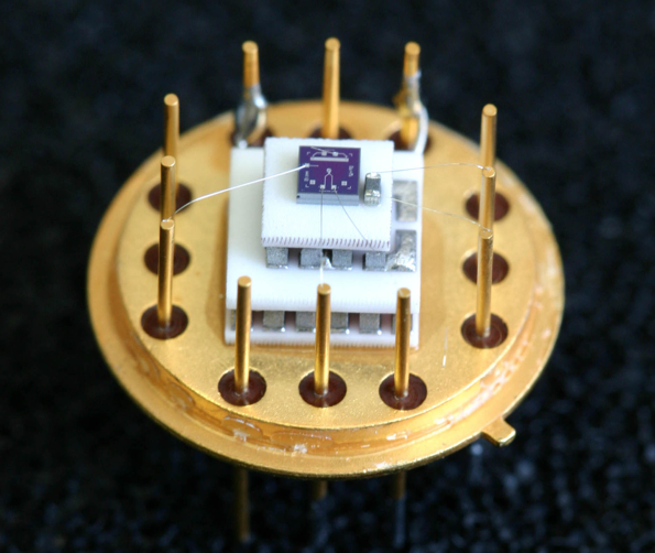
Test of SPAD detectors
Following the fabrication, we extensively characterize our SPADs in the lab, performing various types of measurement to evaluate each figure of merit of the detectors. For example, we developed a fully automated measurement system to precisely measure the quantum efficiency of the detector at the different wavelengths. Moreover, we measure the temporal resolution of SPADs by illuminating the detector with a femtosecond laser and detecting the corresponding pulse with reading electronics developed on purpose. Even more, we can characterize the detector noise down to cryogenic temperatures using a cooling system based on liquid nitrogen. It is worth saying that all these measurements, as well as the many others that have not been mentioned for the sake of conciseness, have a twofold advantage. They not only give us a complete overview of the detector performance, but they also allow us to verify and improve the physical models that describe the behavior of the detector. For these reasons, the experimental phase is always followed by a critical analysis of the data which can lead to the development of new models and/or to the design of new structures.
Current Research Topics
Although the basic principle of SPADs has been present in the literature for a long while now, in recent years there has been a growing interest in these detectors, especially since the exploitation of planar processes made it possible to achieve a high fabrication yield. Nowadays, many aspects of the behavior of these devices still need to be investigated and design margins are wide to come up with new solutions. In particular, the research focus of our lab is currently on the development of SPADs with high quantum efficiency, especially in the near infrared (up to 1µm), combined with high temporal resolution and low noise. Moreover, the fabrication of dense and high-performance linear and bidimensional SPAD arrays would enable unprecedented results in a great variety of applications (see System section). Pushing the performance of SPADs beyond the current limits requires both the development of fine mathematical-physical models (see Modeling section) and the investigation of new device structures to break the current trade-offs.